General Description
The Evaluation Board demonstrates that the RT9490WSC is designed for a highly-integrated 5A Buck-Boost switch mode battery charge management and system power path management device for 2-4 cell Li-Ion and Li-polymer batteries. The low impedance power path optimizes switch-mode operation efficiency, reduces battery charging time, and extends battery life during the discharging phase. The I2C serial interface with charging and system settings makes the device a truly flexible solution.
Performance Specification Summary
Summary of the RT9490WSC Evaluation Board performance specification is provided in Table 1. The ambient temperature is 25°C.
Table 1. RT9490WSC Evaluation Board Performance Specification Summary
|
Specification
|
Test Conditions
|
Min
|
Typ
|
Max
|
Unit
|
|
Supply Input Voltage Range
|
|
3.6
|
--
|
24
|
V
|
|
Maximum Input Current
|
|
--
|
--
|
3.3
|
A
|
|
Maximum OTG Current
|
OTG mode
|
--
|
--
|
3.32
|
A
|
|
Maximum Output Current
|
(SW2), ISYS
|
--
|
--
|
5
|
A
|
|
Maximum Battery Voltage
|
|
--
|
--
|
18.8
|
V
|
|
Maximum Charge Current
|
|
--
|
--
|
5
|
A
|
|
Maximum Discharge Current
|
|
--
|
--
|
10
|
A
|
Detailed Description of Hardware
Headers Description and Placement
Carefully inspect all the components used in the EVB according to the following Bill of Materials table, and then make sure all the components are undamaged and correctly installed. If there is any missing or damaged component, which may occur during transportation, please contact our distributors or e-mail us at evb_service@richtek.com.
Test Points
The EVB is provided with the test points and pin names listed in the table below.
|
Test Point/
Pin Name
|
Function
|
|
VIN1
|
Input voltage for VAC1.
|
|
PGND
|
Ground.
|
|
VIN2
|
Input voltage for VAC2.
|
|
SYSTEM
|
Output voltage for sys.
|
|
BATTERY
|
Battery connection point.
|
|
SNS_BATP
|
External battery positive sense.
|
|
SNS_BATN
|
External battery negitive sense.
|
|
PD1
|
USB Type-C port.
|
|
JP7
|
Type-C USB BUS tied to VAC1 or VAC2 jumper.
|
|
JP9
|
Micro USB BUS tied to VAC1 or VAC2 jumper.
|
|
JP14
|
SDRV tied to ship FET or 1nF capacitor.
|
|
JP19
|
Pull up for I2C/INT/CE.
|
|
JP1
|
ACDRV1 pull-low jumper.
|
|
JP6
|
ACDRV2 pull-low jumper.
|
|
JP4
|
VAC1-VBUS short jumper.
|
|
JP8
|
VAC2-VBUS short jumper.
|
|
JP2
|
USB_D+ jumper.
|
|
JP5
|
USB_D- jumper.
|
|
JP11
|
BAT-BATTERY short jumper.
|
|
JP13
|
BATP tied to drain of ship FET jumper.
|
|
JP16
|
BATP tied to GND or external battery negitive sense jumper.
|
|
JP17
|
BATP tied to BAT pin jumper.
|
|
JP20
|
REGN for TS circuit pull high jumper.
|
|
JP21
|
Test resistence jumper with 500mA for ILIM_HZ function.
|
|
JP22
|
Test resistence jumper with 1.5A for ILIM_HZ function.
|
|
JP23
|
CE pull-low jumper.
|
|
JP25
|
Test resistence jumper with TS_NORMAL for JEITA.
|
|
JP26
|
Test resistence jumper for with TS_POTENTIOMETER JEITA.
|
|
JP27
|
Test resistence jumper for ILIM_HZ function
|
|
JP28
|
PG_LED enable jumper.
|
|
JP29
|
STAT_LED enable jumper.
|
|
JP35
|
This header is for part number RT9490S.
|
|
JP36
|
This header is for part number RT9490S.
|
|
JP37
|
PROG resistence jumper for default set 2S_1.5MHz_2A ICHG.
|
|
JP38
|
PROG resistence jumper for default set 2S_750KHz_2A ICHG.
|
|
JP39
|
PROG resistence jumper for default set 3S_1.5MHz_1A ICHG.
|
|
JP40
|
PROG resistence jumper for default set 3S_750KHz_1A ICHG.
|
|
JP41
|
PROG resistence jumper for default set 4S_1.5MHz_1A ICHG.
|
|
JP42
|
PROG resistence jumper for default set 4S_750KHz_1A ICHG.
|
|
CP2
|
VAC1-VBUS short pad.
|
|
CP3
|
VAC2-VBUS short pad.
|
|
CP9
|
BAT-BATTERY short pad.
|
|
S1
|
Button for exit ship mode or system reset.
|
Default Jumper Setting on EVB
|
Jumper
|
Description
|
|
JP1
|
Short ACDRV1 to _acdrv1.
|
|
JP6
|
Short ACDRV2 to _acdrv2.
|
|
JP13
|
Short BATP to BATTERY.
|
|
JP14
|
Short SDRV to MOS.
|
|
JP16
|
Short BATN to GND.
|
|
JP20
|
Short REGN to TS pull-up resistor.
|
|
JP25
|
Short TS to normal temperature resistor.
|
|
JP22
|
Short ILIM for 1.5A.
|
|
JP37
|
For 2 cell/1.5MHz setting.
|
Quick Start Procedure
Suggestion Required Equipments
- RT9490WSC Evaluation Board
- DC power supply capable of 24V, 3.3A
- Battery simulator capable of 18.8V, 10A
- Electronic load capable of 10A
- Oscilloscope
Evaluation Board Jumper Setup
The Evaluation Board is fully assembled and tested. Follow the steps below to verify board operation. Do not turn on supplies until all connections are made. When measuring the output voltage ripple, care must be taken to avoid a long ground lead on the oscilloscope probe. Measure the output voltage ripple by touching the probe tip and ground ring directly across the last output capacitor.
1. Use jumpers on JP37 to JP42 to set battery cells and switching frequency for default charging profile.
|
Battery Cell (s)
|
Switching Frequency
|
Jumper No.
|
|
2S
|
1.5MHz
|
JP24
|
|
750kHz
|
JP25
|
|
3S
|
1.5MHz
|
JP26
|
|
750kHz
|
JP27
|
|
4S
|
1.5MHz
|
JP28
|
|
750kHz
|
JP29
|
2. Use jumpers on JP1 and JP6 to connect ACDRV1 and ACDRV2 to the gate driver output from IC. If the external AC-RBFETs are not needed, use jumpers on JP4 and JP8 to bypass them and JP1 and JP6 should be used to connect ACDRV1 and ACDRV2 to GND.
3. Use a jumper on JP14 with Mid-Right side to connect SDRV to the gate driver output from IC. If the external ship FET is not needed, use a jumper on JP11 to bypass it and use JP14 with Mid-Left side to connect SDRV to the capacitor.
4. Use a jumper on JP25 (TS_NORMAL) or JP26 (TS_POTENTIOMETER) for setting TS pin configuration and JP20 for connecting to REGN as pull-up voltage.
5. Use a jumper on JP21 (500mA) or JP22 (1.5A) for ILIM setting and JP27 for controlling HIZ_EN.
6. Use a jumper on JP16 to connect BATN to PGND.
7. Use a jumper on JP13 for connecting BATTERY to BATP when the external ship FET is adopted.
8. Use a jumper on JP17 for connecting BAT to BATP when the external ship FET is not adopted.
9. Use a jumper on JP9 for connecting Type_C_IN on VAC1 or VAC2.
Proper measurement equipment setup and follow the procedure below.
1. With power off, connect input power and ground to VIN1 or VIN2 and PGND respectively.
2. With load off, connect electronic load to SYSTEM and PGND respectively.
3. With power off, connect power and ground to BATTERY and PGND respectively. Turn on battery simulator, then the device is powered up.
4. Use I2C to set registers for charging function and proper protection level. Richtek also provides designers GUI software tool to read or write registers. The details are shown in the next chapter ” Evaluation GUI Software Tool Installation and Introduction”.
5. Turn on the input power supply to start charging. Make sure that the power supply voltage is under OVP level.
6. Check the output charging current using a current meter.
7. Once the proper charging current is established observe the output voltage regulation, ripple voltage, efficiency and other performance.
8. For testing SYS load, turns on the electronic load and adjusts SYS current.
Evaluation GUI Software Tool Installation and Introduction
The function settings of the RT9490 are not only hardware pins but also software register settings. The RT9490 register is set via I2C communication. To test evaluation board conveniently, Richtek provides GUI tool and users can use it to read and write the register. Follow the below steps to install the relative software tools.
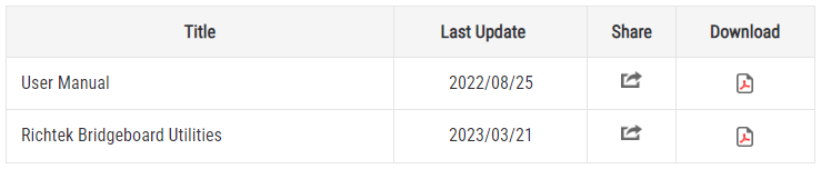
1. Richtek Bridgeboard Utilities Installation
Get the Richtek Bridgeboard Utilities, user manual and purchase the bridge board from the website.
https://www.richtek.com/Design%20Support/Reference%20Design/RD0001-01?sc_lang=en
Please follow the user manual to install the Richtek Bridgeboard Utilities.
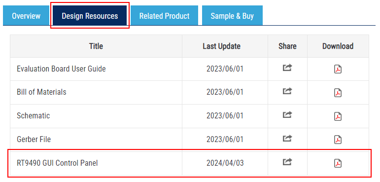
2. Download the GUI
Get the RT9490 GUI from website.
https://www.richtek.com/Design%20Support/Reference%20Design/UG9490WSC?sc_lang=en
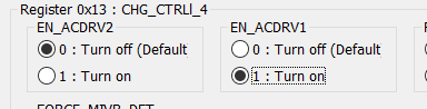
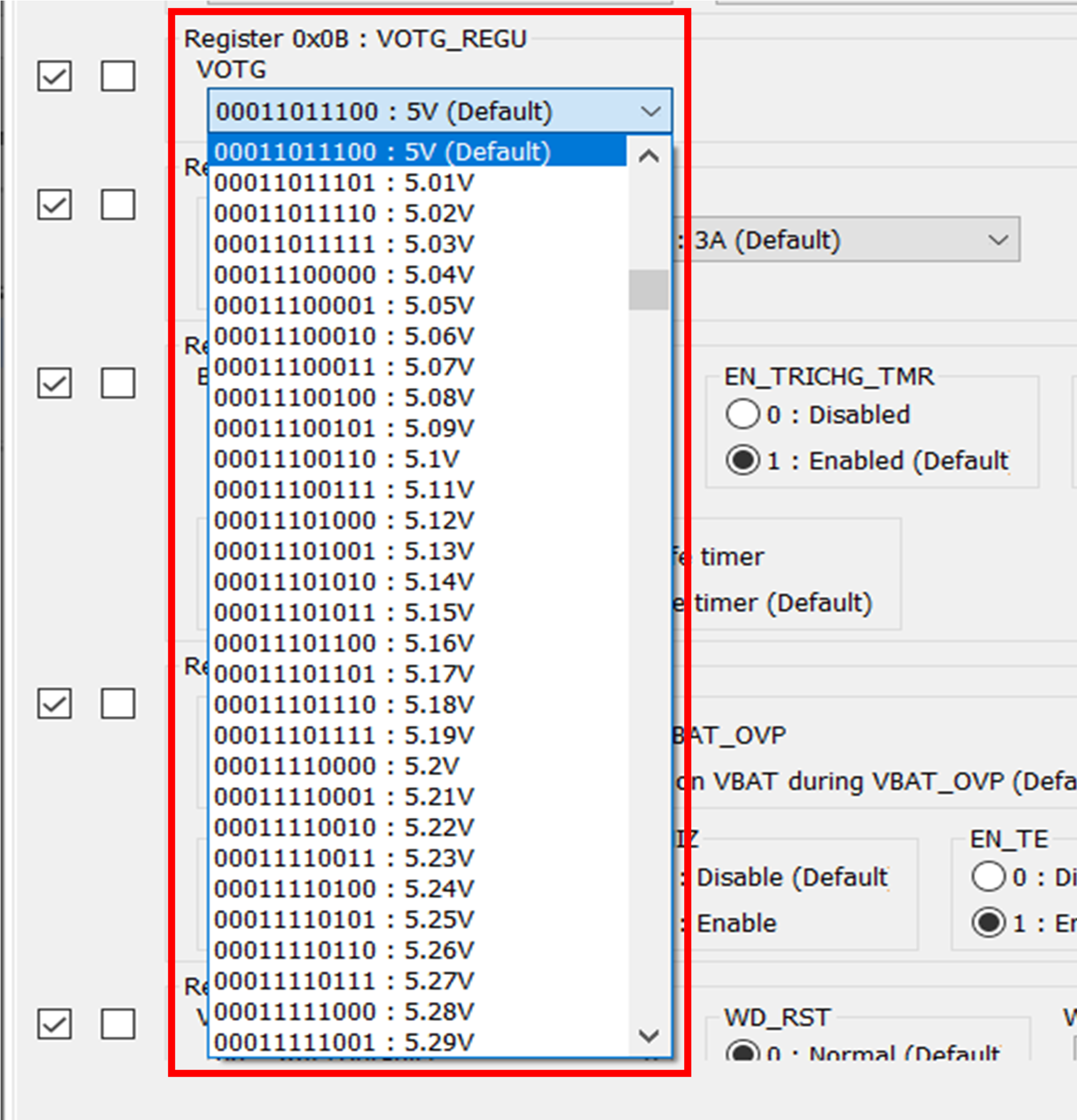
3. The introduction of GUI interface is as below.
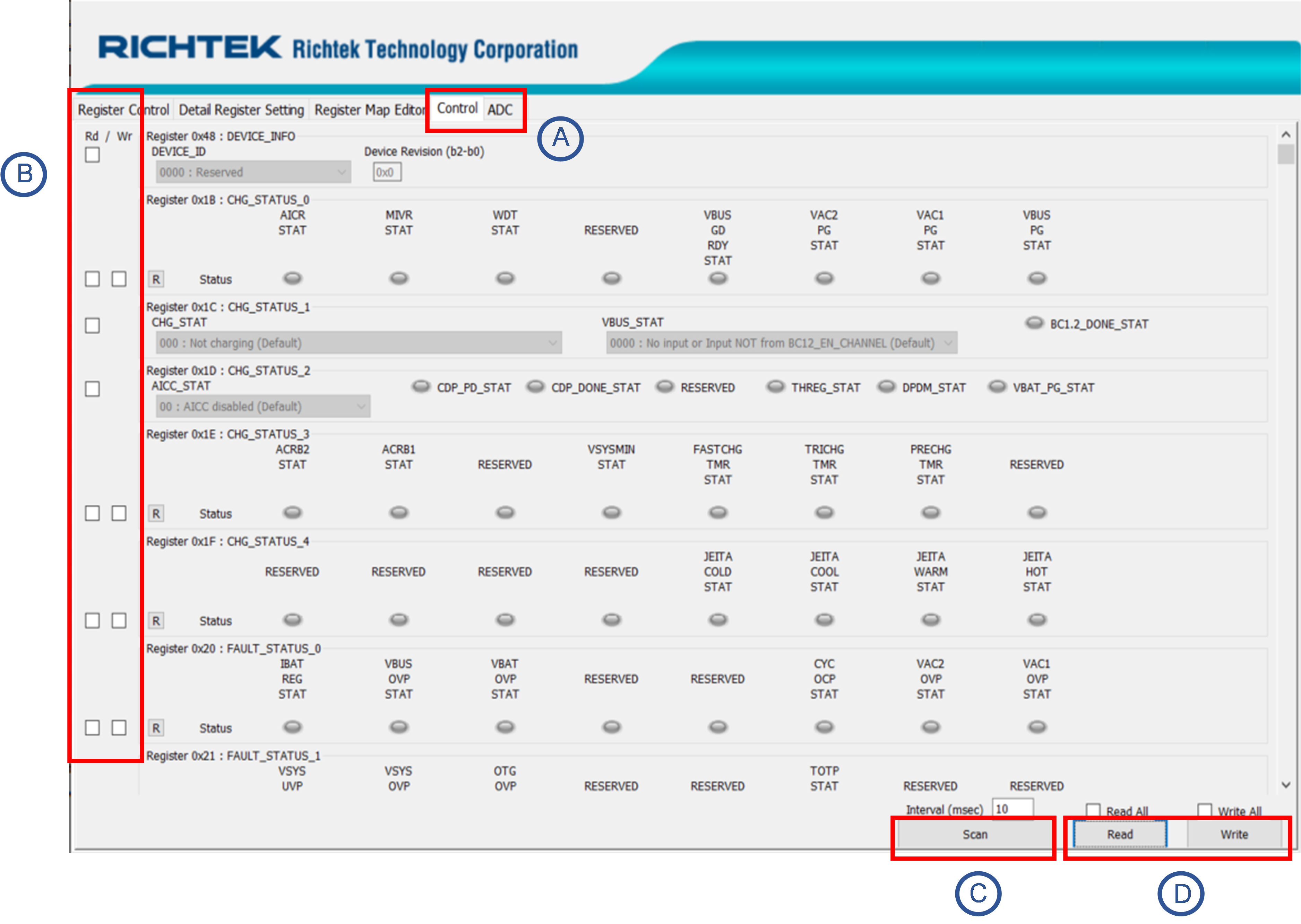
A:
All registers can be read/written in these pages.
B:
You can select which byte you want to read/write in this column.
C:
The selected register will continue to be read after click the scan button.
D:
Write: The selected register will be written to the device after click the write button.
Read: The selected register will be updated after click the read button.
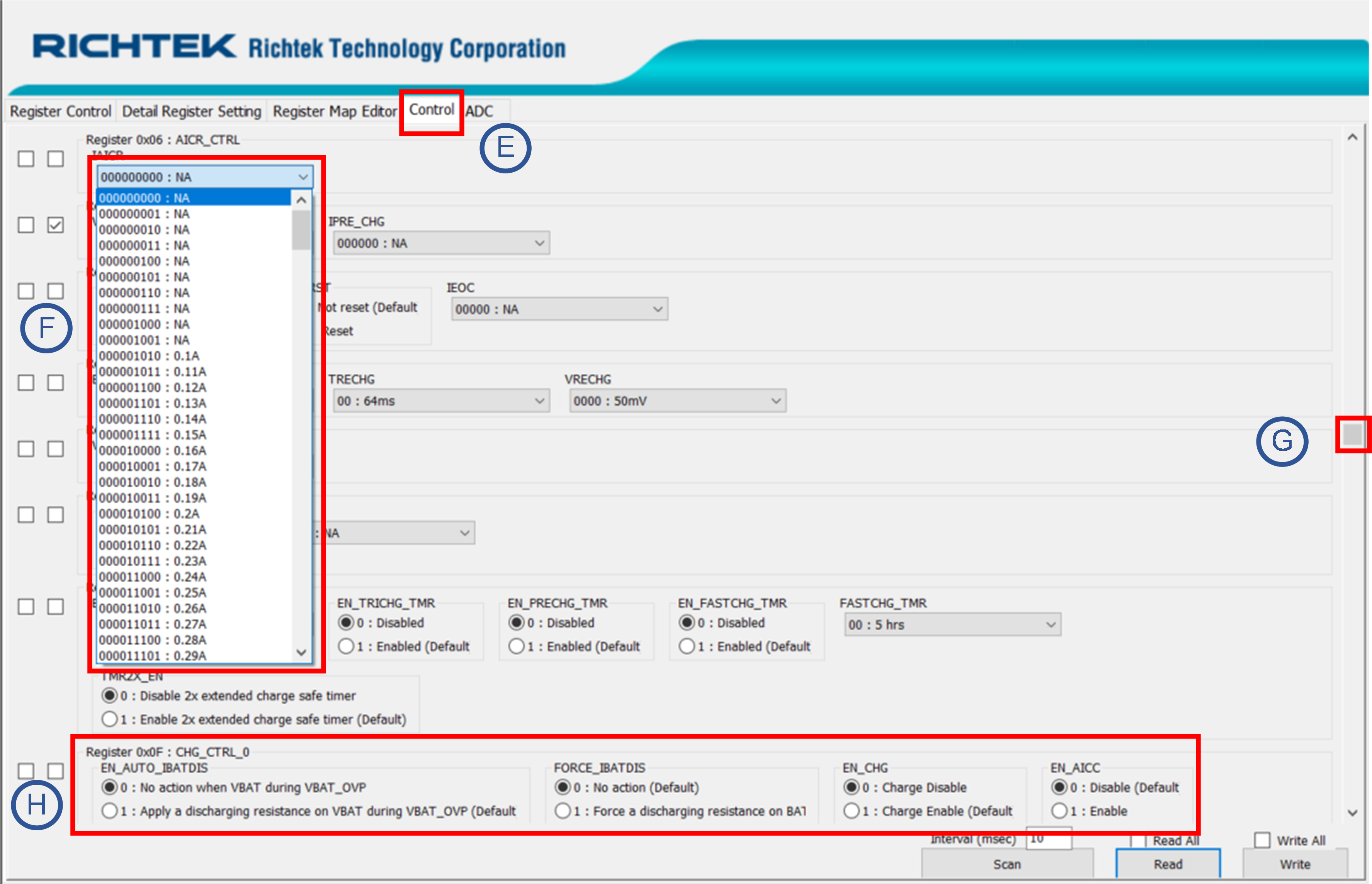
E:
This page is for charging behavior setting.
F:
This type of dropdown menu allows you to select the setting you need.
G:
You can scroll down/up to select the register setting.
H:
This type of menu allows you to select the bit setting you need. A solid fill indicates your selection.
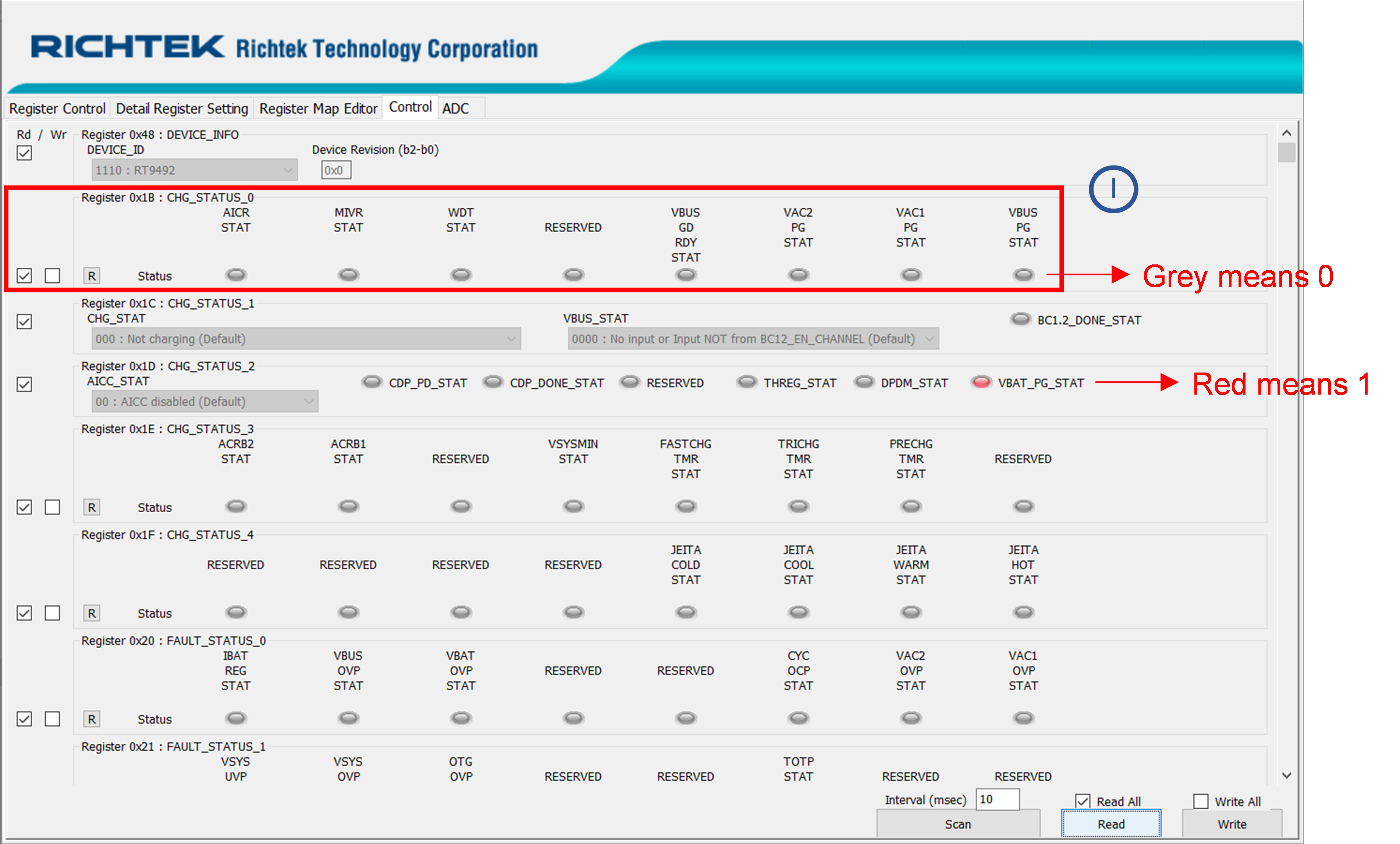
I:
These lamp icon are STATUS type of register.
Test Procedure
Hardware Initial Settings
1. Follow the section “Evaluation Board Jumper Setup” to set the board jumper.
2. Use a battery simulator or a real battery to power up the RT9490 at the BATTERY pin. The voltage should be within the application range. For example, in 2-cell application, users can initially provide 8V to the BATTERY pin.
GUI Setup
1. Follow the section” Evaluation GUI Software Tool Installation” to Install the GUI tool.
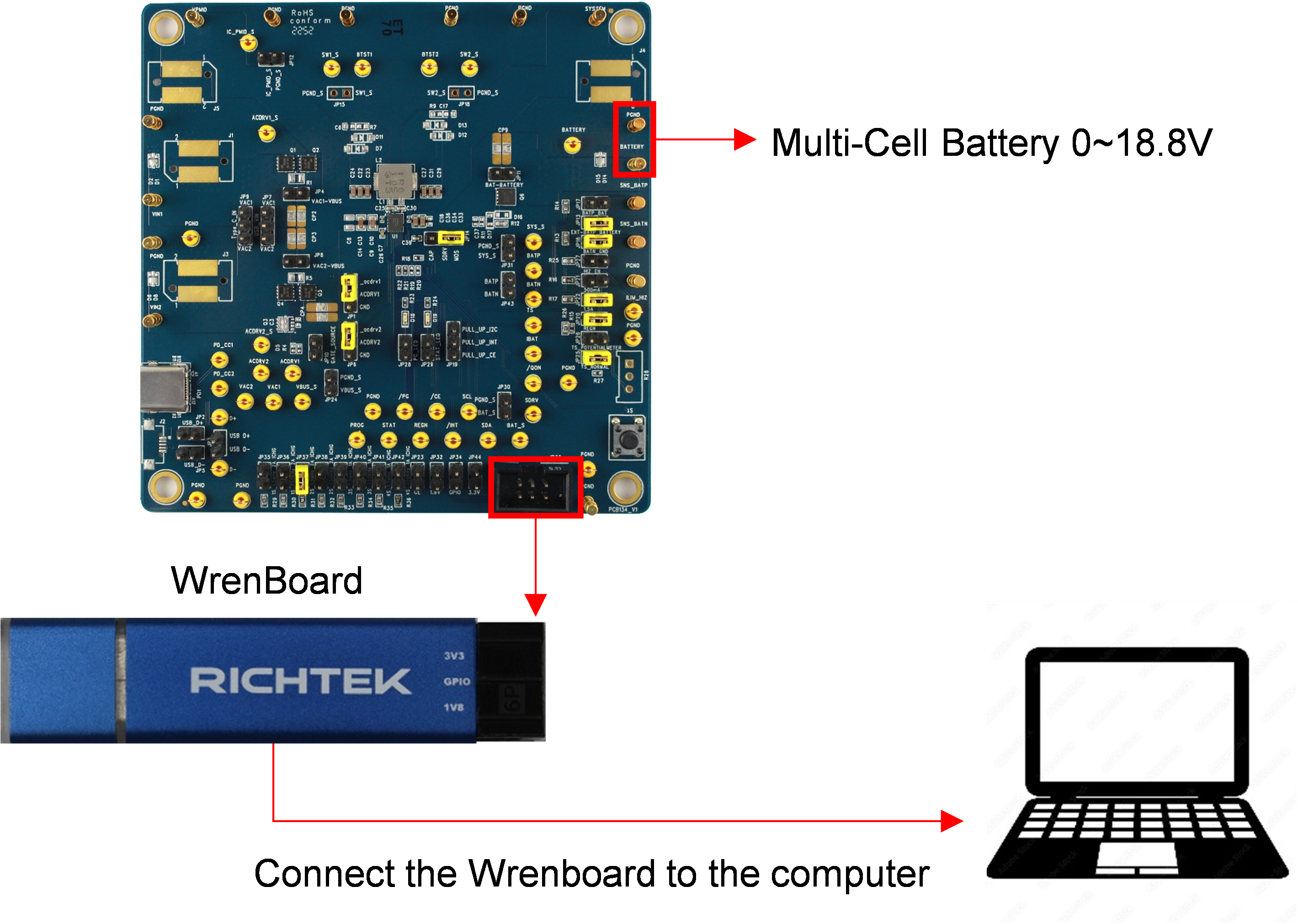
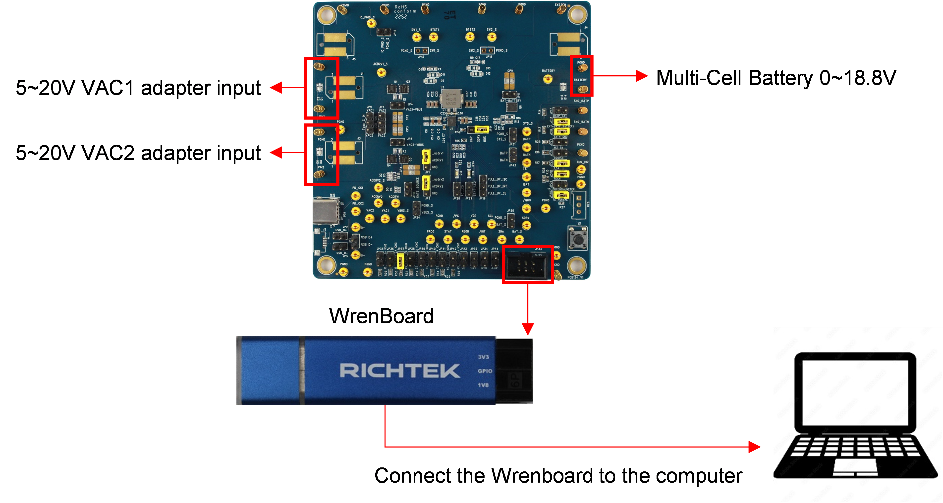
2. Connect Richtek Wrenboard to evaluation board through JP33 SCL/SDA/PGND pin.
3. Connect Richtek Wrenboard to the computer.
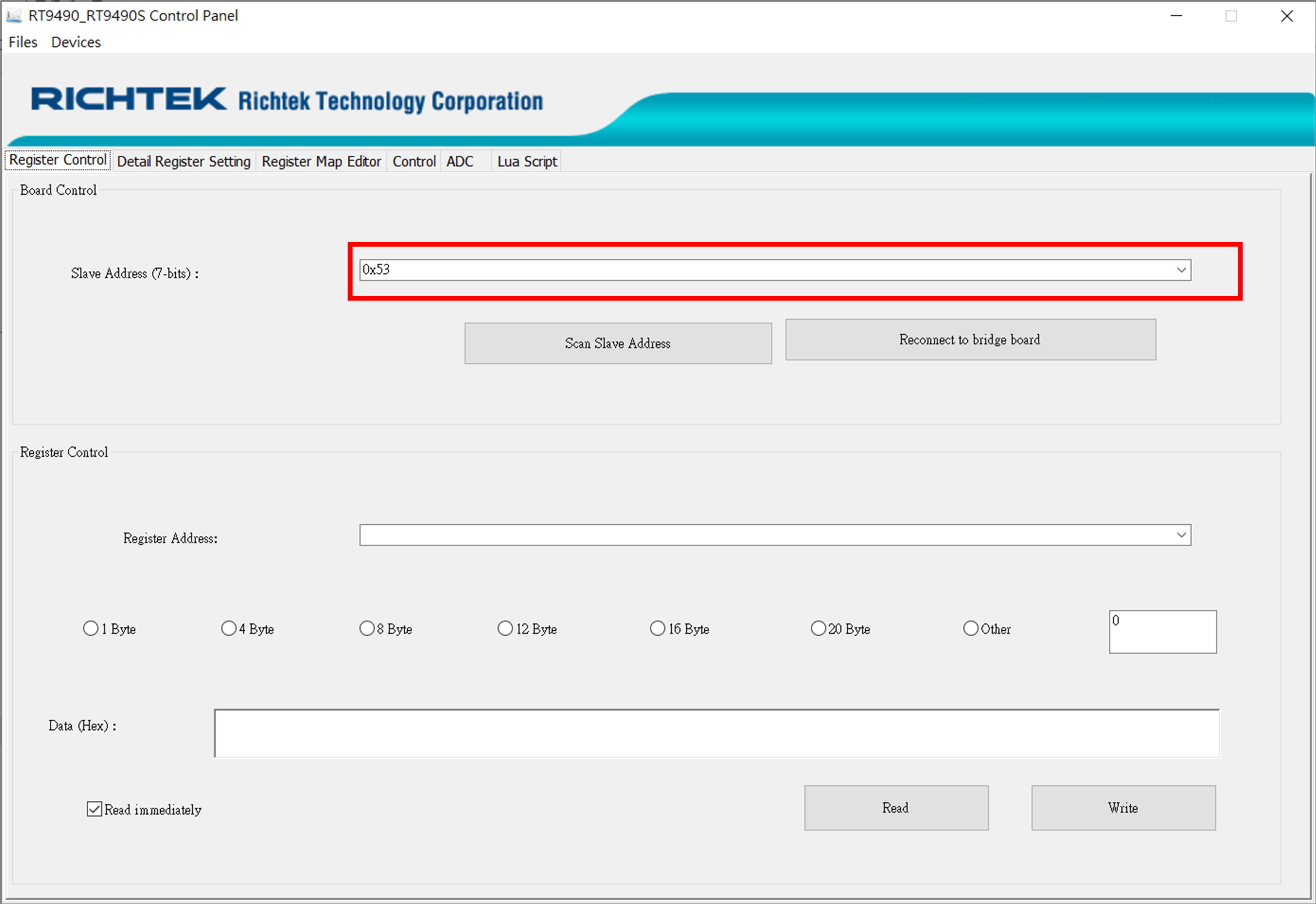
4. After providing power to the Evaluation Board, run the RT9490_RT9490S_GUI_V4.exe.
5. If GUI connection is successful, the slave address ID will show 0x53.
Register Initial Setting
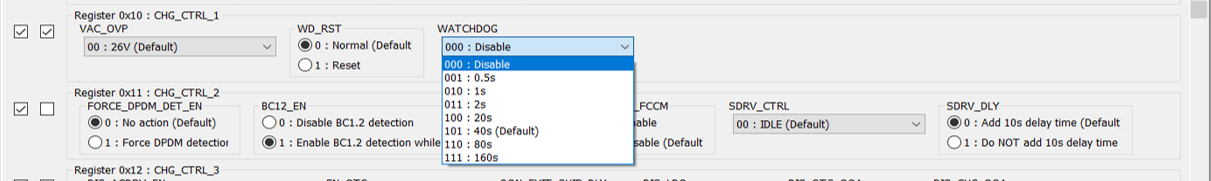
1. For board evaluation, disable watchdog initially if don’t want to verify watchdog function.
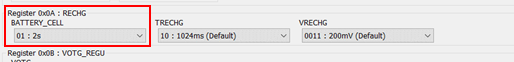
2. Check whether BATTERY_CELL setting is the same as PROG pin setting. This register can also be changed after powered up.
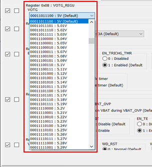
3. Set VSYSMIN for Buck-Boost sys pin minimum regulation level. Set it as minimum system voltage.
4. Set VBAT_REG for battery full charged level.
5. Set ICHG_CTRL for fast charge current level.
6. Set VMIVR for input voltage limitation level. Set it lower than test input voltage.
7. Set IAICR for input current limitation level. Set it lower than test input source current limit.
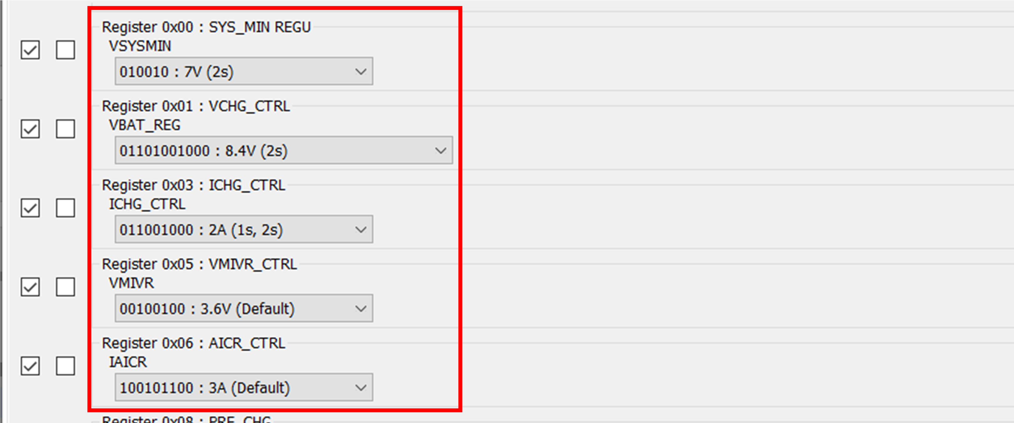
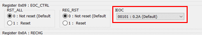
8. Set the IEOC for charging termination level.
9. Check whether VAC_OVP level is large enough. It should bigger than VBUS input voltage.
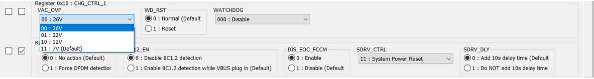
10. The charger input current limit is decided by the minimum value between AICR and ILIM. If do not want to verify the ILIM_HZ function, disabled ILIM_HZ function.

Charger Function Test
1. After finishing register initial setting, give VAC1 or VAC2 pin input power to start charger. For example, give it 15V.
2. Check whether it triggers AICR_STAT, MIVR_STAT, or other protections.
3. If it triggers AICR_STAT, it means that the input current is near limitation level. Increase input voltage or reduce ICHG_CTRL setting to leave AICR_STAT.
4. If it triggers MIVR_STAT, it means that the input power is not enough and input source voltage drops. Increase input power ability or reduce ICHG_CTRL setting to leave MIVR_STAT.
5. Check the CHG_STAT. In CC mode, the charging current will be regulated as register ICHG_CTRL if it doesn’t have AICR_STAT and MIVR_STAT.
6. Measure the BAT pin output current to verify the fast charge current.
7. Gradully increase battery simulator voltage to simulate battery charging.
8. Measure the charging current and the BATP pin voltage as the battery voltage increases. Once the charging current starts to fall down, verify that the voltage remains at the VBAT_REG level (IR drop + VBAT = VBAT_REG level).
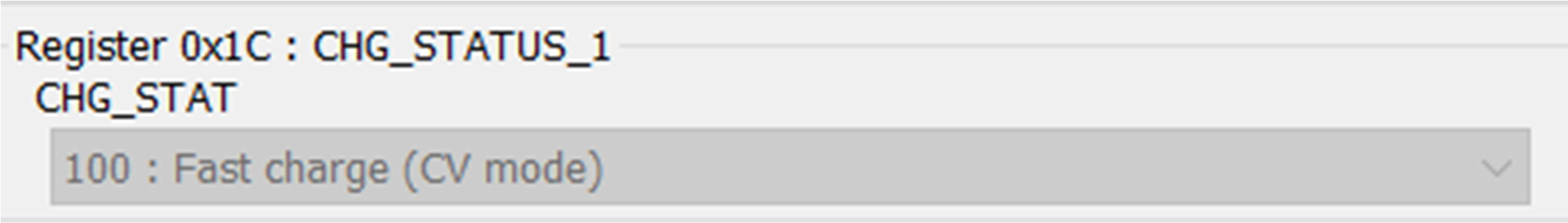
9. Check that CHG_STAT is into CV mode.

10. Continue increasing the battery voltage. Check that the BAT charging current is gradually down in CV mode.
11. After BAT charging current is below IEOC level, the RT9490 will stop charging.
12. CHG_STAT will show Charge_done at this full-charged stage.
13. If EN_TE is disabled at initial setting, the IEOC function will not work at this stage. The RT9490 will not stop charging and will continue charging until the current decreases to 0A.
14. To verify the recharge function, load the SYS pin to discharge the battery or reduce the voltage of the battery simulator.
15. The recharge level is determined by the VRECHG register.
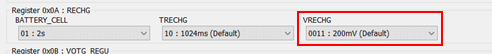
16. Afrer battery voltage is below (VBAT_REG-VRECHG), the RT9490 will start to charge again. For example, VBAT_REG is 8.4V, VRECHG is 200mV and the recharge level will be 8.2V.
17. Plug out the VAC input power. RT9490 will stop charging.
OTG Function Test
1. Finish register initial setting as section” Register initial setting” .
2. Make sure the battery voltage is above VOTG_LBP (typ. 2.7V). For example, provide it 8V.
3. Set the OTG voltage level.
4. Enable EN_OTG. The RT9490 will start to output voltage at the VBUS pin.
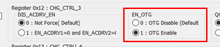
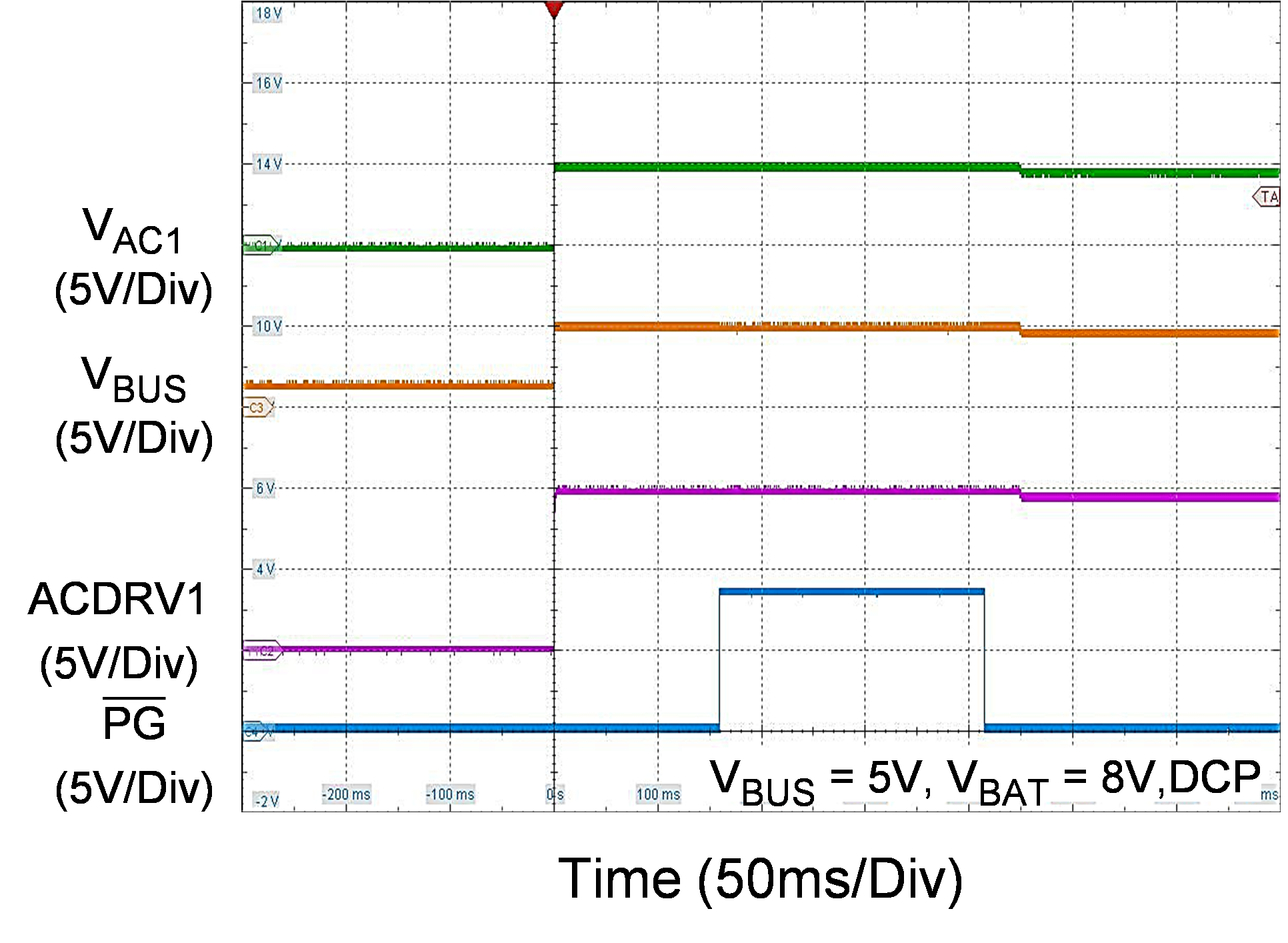
5. On the RT9490 evaluation board, there are mounted AC-RBFETs already. If AC-RBFET is used by jumper setting(see the details in the section” Evaluation Board Jumper Setup”), OTG only starts after the choosed AC-RBFET is turned on.
For example, if VAC1 RBFET is used, EN_ACDRV1 should be enabled. The RT9490 starts to output OTG voltage after register EN_ACDRV1 is set to 1.
6. Measure the VBUS pin and VAC pin to verify the OTG setting level.
7. After OTG starts, OTG voltage is still able to be set.
Measure Results Reference
|
Power Up with VAC Pluged in
|
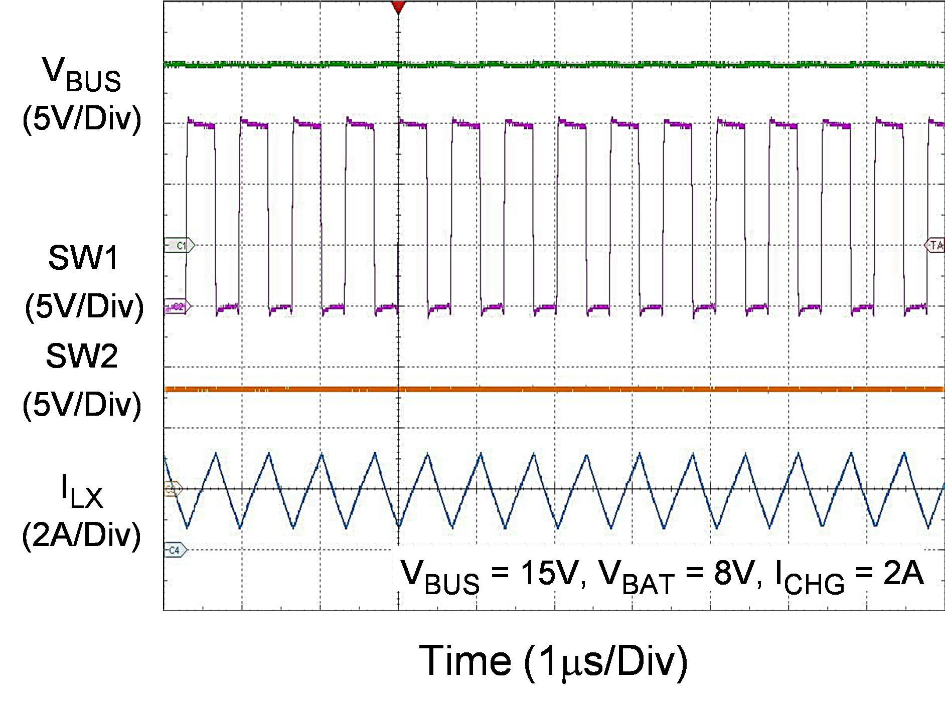
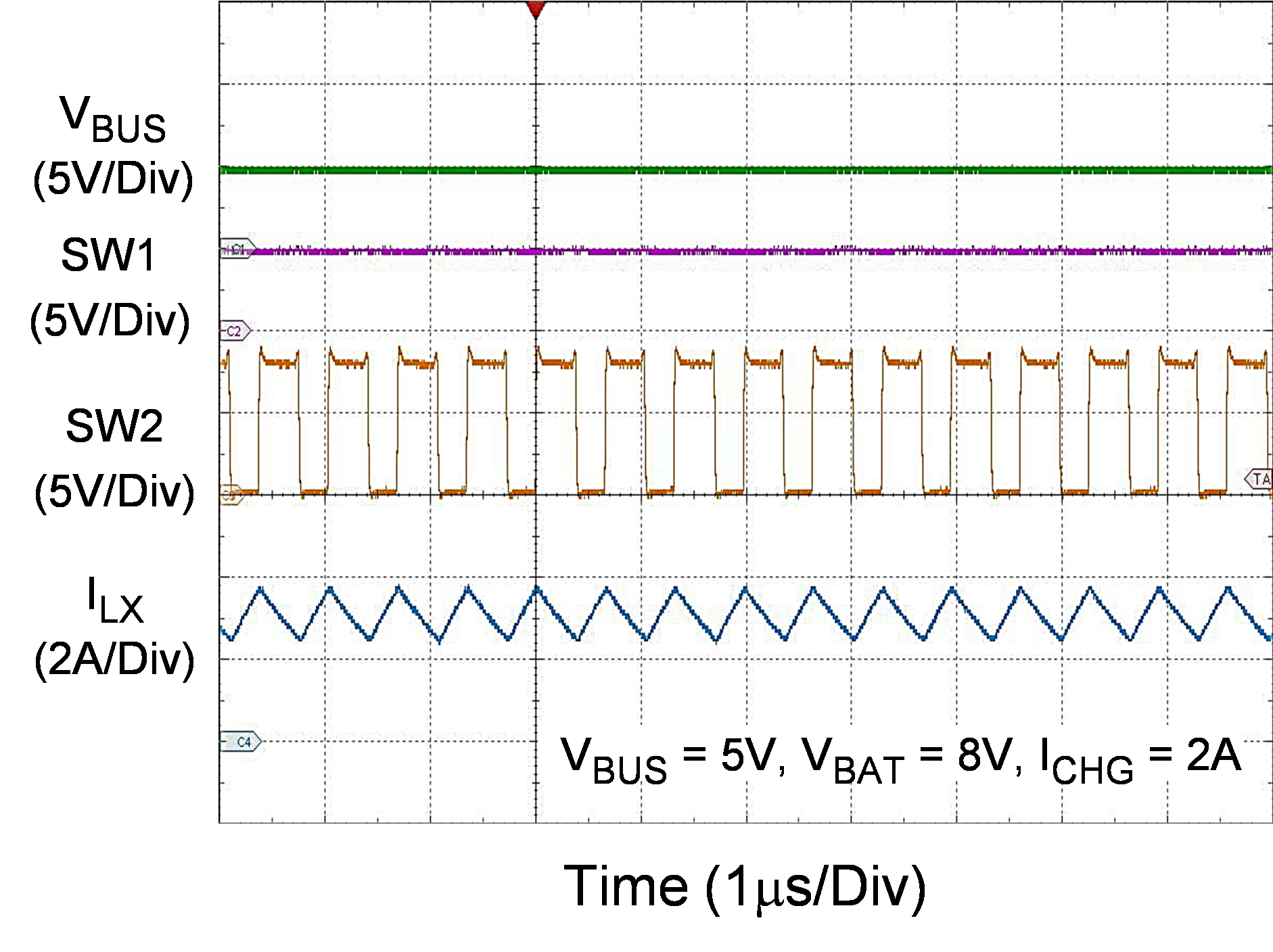
Charging in Buck Mode
|
|
|
|
|
Charging in Boost Mode
|
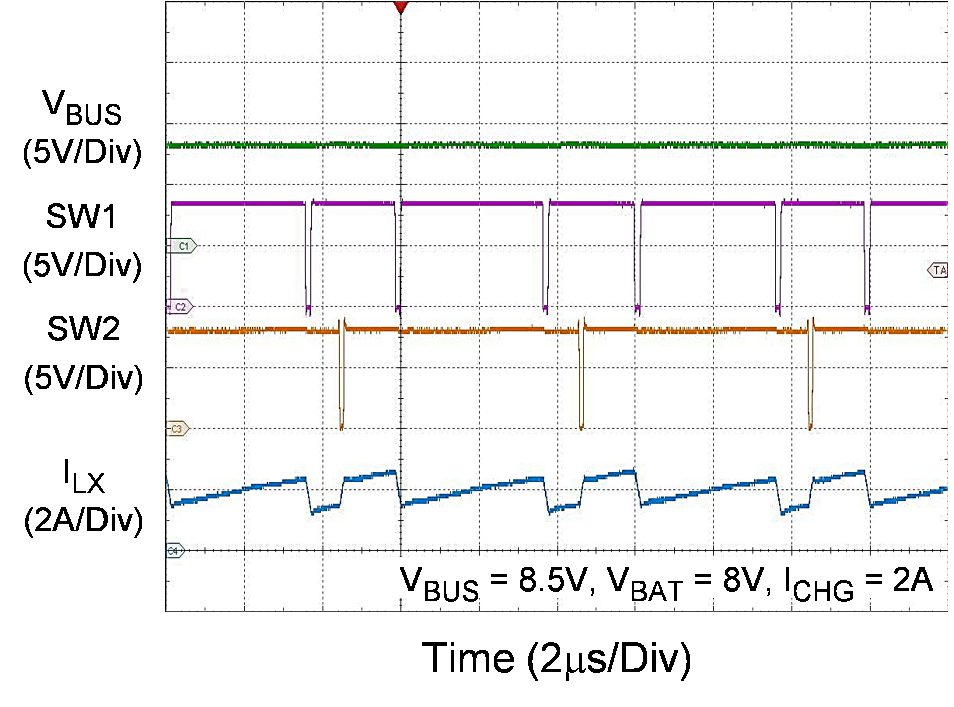
Charging in Buck-Boost Mode
|
|
|
|
|
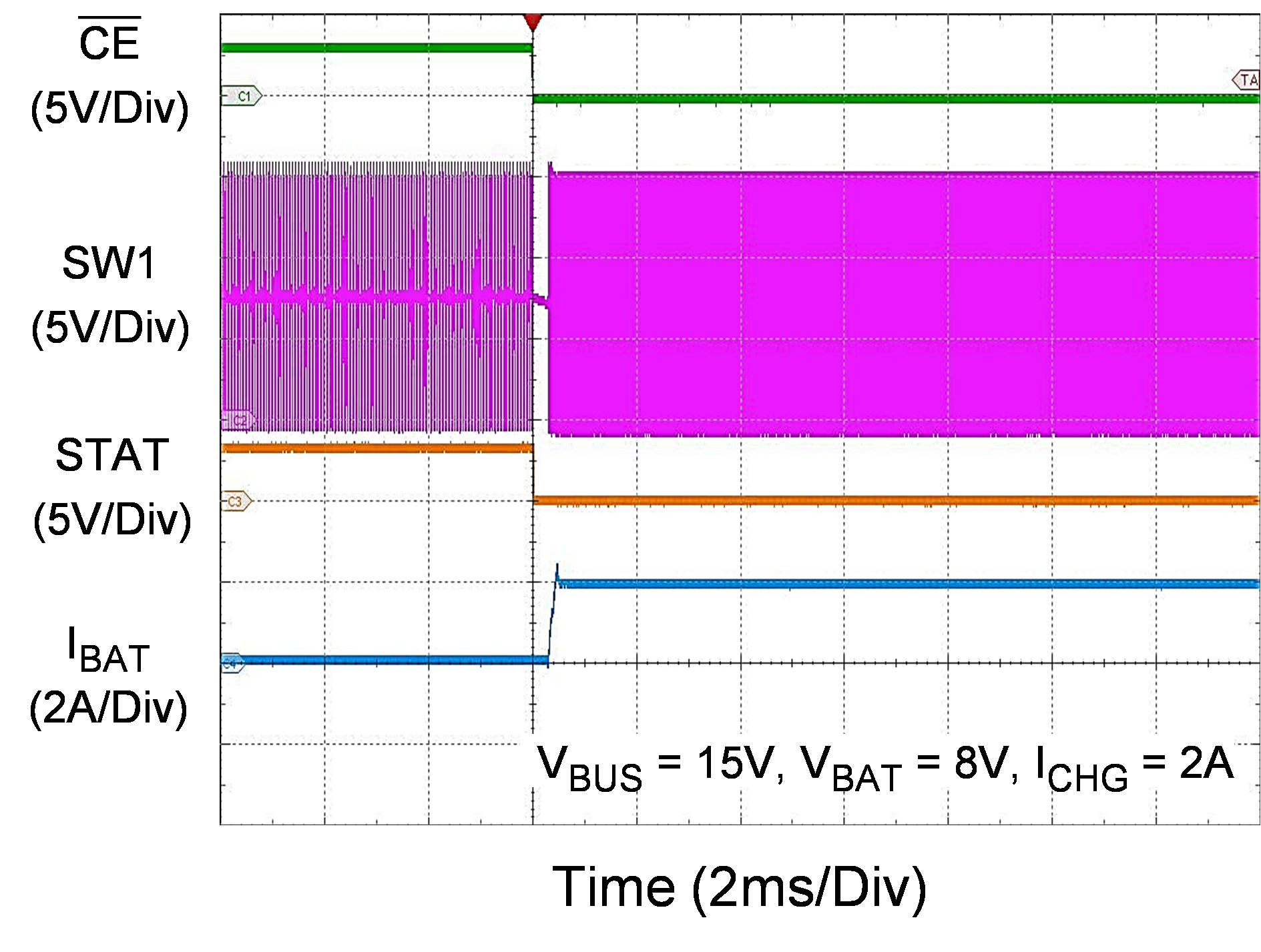
Charging Enabled by CE Pin
|
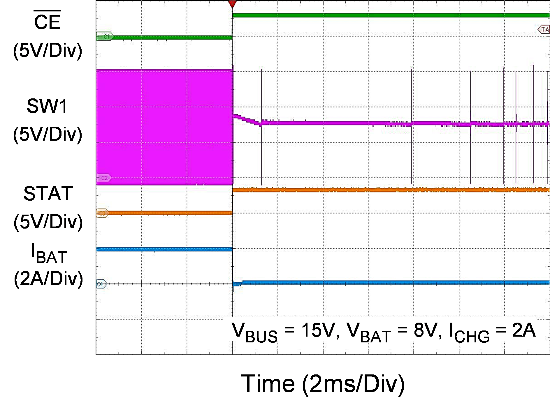
Charging Disabled by CE Pin
|
|
|
|
|
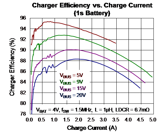
1s Battery Charger Efficiency
|
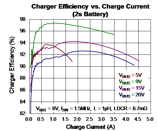
2s Battery Charger Efficiency
|
|
|
|
|
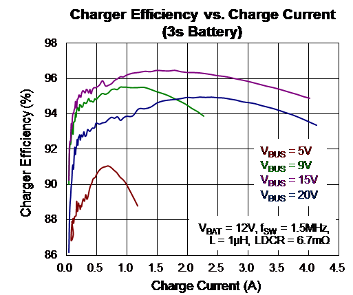
3s Battery Charger Efficiency
|
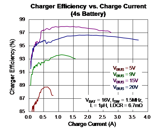
4s Battery Charger Efficiency
|
|
|
|
|
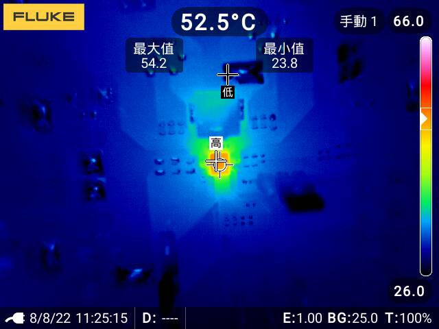
Thermal Image at VIN = 15V, VBAT = 8V, ICHG = 2A
|
|
|
Note: When measuring the input or output voltage ripple, care must be taken to avoid a long ground lead on the oscilloscope probe. Measure the output voltage ripple by touching the probe tip directly across the output capacitor.
Typical Applications
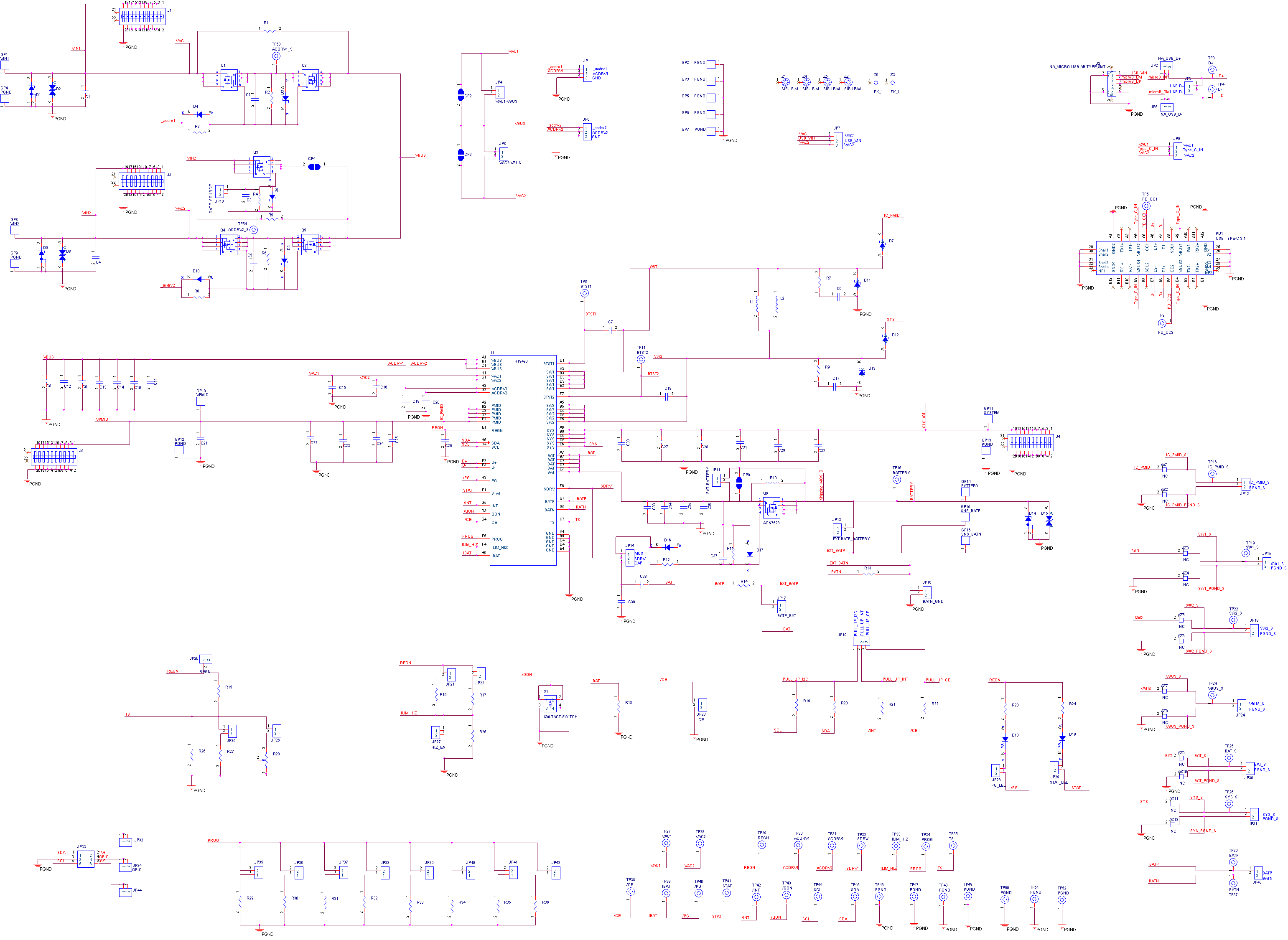
EVB Schematic Diagram
Bill of Materials
|
fSW = 1.5MHz
|
|
Reference
|
Count
|
Part Number
|
Value
|
Description
|
Package
|
Manufacturer
|
|
U1
|
1
|
RT9490WSC
|
--
|
Switching Charger
|
WL-CSP-56B 2.93x3.46 (BSC)
|
RICHTEK
|
|
C7, C18
|
2
|
GRM033R61C473KE84
|
47nF
|
Capacitor, Ceramic, 16V, X5R
|
C-0201
|
MURATA
|
|
C10, C13, C22, C23, C24
|
5
|
GRM188R6YA106MA73
|
10µF
|
Capacitor, Ceramic, 35V, X5R
|
C-0603
|
MURATA
|
|
C11, C25, C30
|
3
|
0402B104K500CT
|
0.1µF
|
Capacitor, Ceramic, 50V, X7R
|
C-0402
|
WALSIN
|
|
C26
|
1
|
GRM155R60J475ME47D
|
4.7µF
|
Capacitor, Ceramic, 6.3V, X5R
|
C-0402
|
MURATA
|
|
C27, C29, C31, C34, C36
|
5
|
GRM188R61E106MA73
|
10µF
|
Capacitor, Ceramic, 25V, X5R
|
C-0603
|
MURATA
|
|
C39
|
1
|
0402B102K500CT
|
1nF
|
Capacitor, Ceramic, 50V, X7R
|
C-0402
|
WALSIN
|
|
D18, D19
|
2
|
LNL-190SUG
|
--
|
LED_GREEN
|
LED-0603
|
LighTop
|
|
L2
|
1
|
PIMB063T-1R0MS-68
|
1µH
|
20%/6.7mΩ
|
L-7-4X6-8
|
CYNTEC
|
|
PD1
|
1
|
121U-3CST-09CR
|
--
|
USB TYPE-C 3.1
|
9.87x9.75mm
|
JEM
|
|
Q1, Q2, Q4, Q5
|
4
|
AONR36366
|
--
|
AONR36366
|
DFN 3x3 EP
|
ALPHA & OMEGA SEMICONDUCTOR
|
|
Q6
|
1
|
AON7528
|
--
|
AON7528
|
DFN 3.3x3.3 EP
|
ALPHA & OMEGA SEMICONDUCTOR
|
|
R12
|
1
|
WR06X000 PTL
|
0
|
Resistor, Chip, 1/10W, 1%
|
R-0603
|
WALSIN
|
|
R13, R14
|
2
|
WR06X1000FTL
|
100
|
Resistor, Chip, 1/10W, 1%
|
R-0603
|
WALSIN
|
|
R15
|
1
|
CR-02FL6---5K1
|
5.1k
|
Resistor, Chip, 1/16W, 1%
|
R-0402
|
VIKING
|
|
R16
|
1
|
RTT032553FTP
|
255k
|
Resistor, Chip, 1/10W, 1%
|
R-0603
|
RALEC
|
|
R17
|
1
|
WR06X1273FTL
|
127k
|
Resistor, Chip, 1/10W, 1%
|
R-0603
|
WALSIN
|
|
R18, R21, R22, R27
|
4
|
WR04X1002FTL
|
10k
|
Resistor, Chip, 1/10W, 1%
|
R-0402
|
WALSIN
|
|
R23, R24
|
2
|
CR-02FL6---4K7
|
4.7k
|
Resistor, Chip, 1/16W, 1%
|
R-0402
|
VIKING
|
|
R25
|
1
|
WR06X1003FTL
|
100k
|
Resistor, Chip, 1/10W, 1%
|
R-0603
|
WALSIN
|
|
R26
|
1
|
WR06X3012FTL
|
30.1k
|
Resistor, Chip, 1/10W, 1%
|
R-0603
|
WALSIN
|
|
R29
|
1
|
RTT033001FTP
|
3k
|
Resistor, Chip, 1/10W, 1%
|
R-0603
|
RALEC
|
|
R30
|
1
|
WR06X4701FTL
|
4.7k
|
Resistor, Chip, 1/10W, 1%
|
R-0603
|
WALSIN
|
|
R31
|
1
|
RC0603FR-076K04L
|
6.04k
|
Resistor
|
R-0603
|
YAGEO
|
|
R32
|
1
|
WR06X8201FTL
|
8.2k
|
Resistor, Chip, 1/10W, 1%
|
R-0603
|
WALSIN
|
|
R33
|
1
|
WR06X1052FTL
|
10.5k
|
Resistor, Chip, 1/10W, 1%
|
R-0603
|
WALSIN
|
|
R34
|
1
|
WR06X1372FTL
|
13.7k
|
Resistor, Chip, 1/10W, 1%
|
R-0603
|
WALSIN
|
|
R35
|
1
|
WR06X1742FTL
|
17.4k
|
Resistor, Chip, 1/10W, 1%
|
R-0603
|
WALSIN
|
|
R36
|
1
|
WR06X2702FTL
|
27k
|
Resistor, Chip, 1/10W, 1%
|
R-0603
|
WALSIN
|
|
S1
|
1
|
HTS6601H
|
--
|
SW-TACT-SWITCH
|
TACT-BTN
|
High-Tronics
|
Evaluation Board Layout
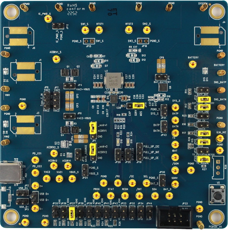
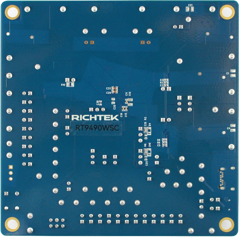
Figure 1 to Figure 4 are RT9490WSC Evaluation Board layout. This board size is 101.6mm x 101.6mm and is constructed on four-layer PCB, outer layers with 1 oz. Cu and inner layers with 1 oz. Cu.
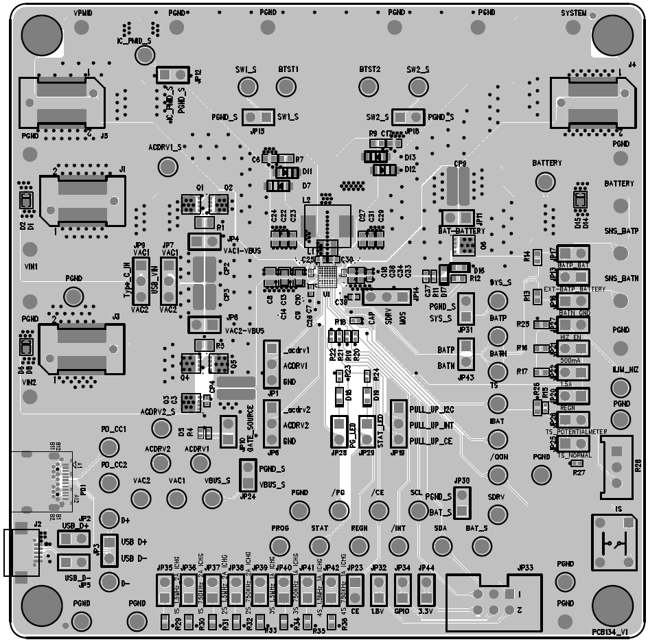
Figure 1. Top View (1st layer)
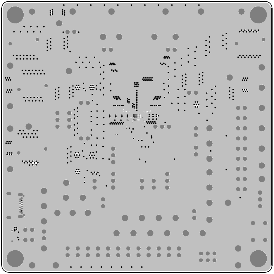
Figure 2. PCB Layout—Inner Side (2nd Layer)
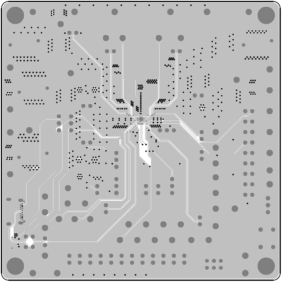
Figure 3. PCB Layout—Inner Side (3rd Layer)
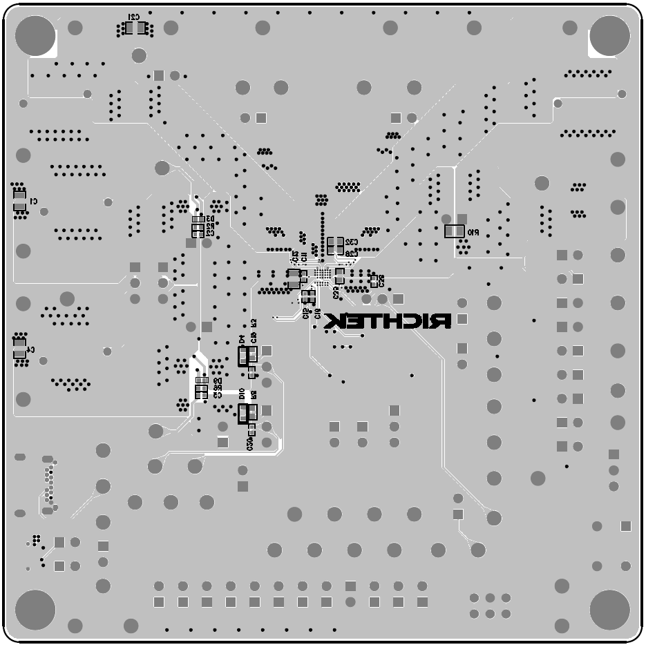
Figure 4. Bottom View (4th Layer)